
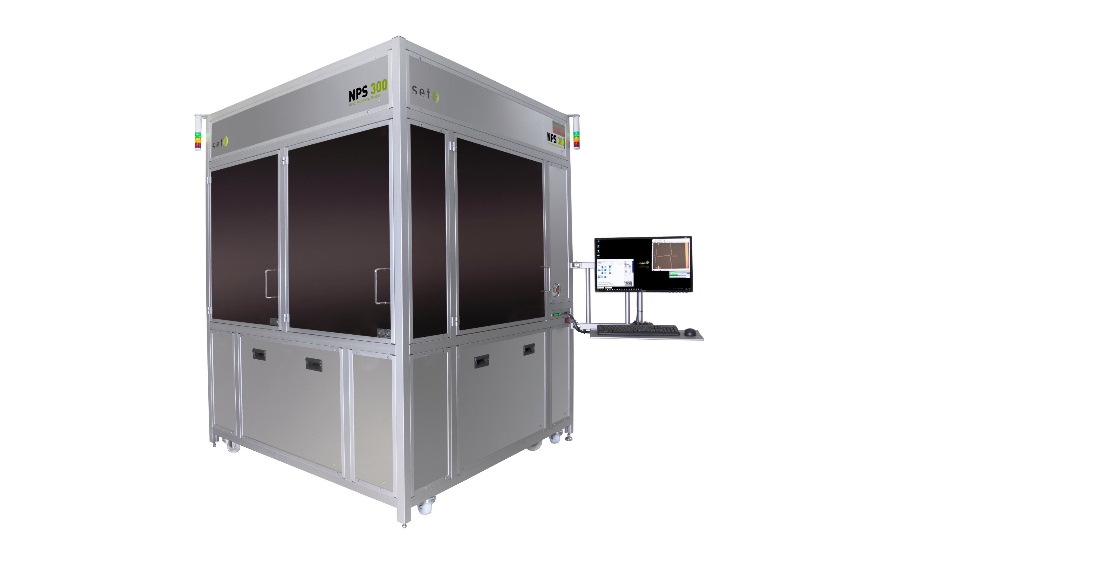
NPS300

Der NPS300 ist auf fortschrittliche Forschung und Entwicklung sowie auf Pilotlinien ausgerichtet und ein Stepper mit hoher Genauigkeit und hoher Kraft, der für das Nanoprägen entwickelt wurde.
Der NPS300 ist für die Replikation von Nanostrukturen mit einer Genauigkeit von ± 0,5 μm optimiert und das erste Werkzeug überhaupt, das ausgerichtete Heißpräge-Lithographie und UV-NIL auf derselben Plattform kombinieren kann.
Der NPS300 ist in der Lage, Geometrien unter 20 nm mit einer Überlagerungsgenauigkeit von 250 nm zu drucken.
Seine flexible Architektur bietet eine hervorragende Prozessreproduzierbarkeit und eine einzigartige Fähigkeit, große Flächen im sequentiellen Step & Repeat-Modus auf Wafern bis zu 300 mm zu strukturieren.
Es ermöglicht die kostengünstige Herstellung großer Stempel mit sich wiederholenden Mustern.

Request the technical paper

  • Hauptvorteile

    • ± 0,5 μm Genauigkeit
    • Step & Repeat-Modus auf Wafern bis 300 mm
    • Automatische Briefmarkenabholung
    • Luftlagertechnologie und Granitstruktur sorgen für langfristige Stabilität und Zuverlässigkeit
    • Kontrolle der Parallelität, um auch bei hohen Kräften eine sehr hohe Genauigkeit zu gewährleisten
    • Freihändige/vollautomatische Kalibrierung
    • Automatischer Zyklus und bedienerunabhängig
    • Hohe Ergiebigkeit durch steifes Design
    • Prozessaufzeichnung für die Entwicklung
    • Protokolldateien zur Nachverfolgung der Produktion
  • Prozessfähigkeiten

    Die Schritt & Prägungsstempel Prägung Lithographie für Heißprägung oder UV-NIL ist ein innovatives Verfahren, das bei der VTT Technical Research Centre in Finnland nachgewiesen wurde.

    • Heißprägung-Lithographie: dieses Verfahren besteht darin, das Stempel-Muster in ein Thermoplast Prägungsmaterial durch Hitze- und Druck-Steuerung zu übertragen
    • UV-NIL: das Verfahren Schritt & Härtung verwendet dosiertes Prägungsmaterial vor Ort und UV-Härtung. Diese innovative Technologie ist eine vielversprechende Lösung, um Standard UV-Lithographie Systeme zu ersetzen, wenn Auflösung unter 20 nm erforderlich ist.
  • Anwendungen

    •  Photonische Geräte
    •  Mikrooptische hochgenaue Arrays und Gitter
    •  CMOS-MEMS Integration
    •  OLED Displays mit Hochauflösung
    •  HDD mit hoher Dichte für mobilen Speicher
    •  Andere neuen Techniken
  • NIL Verfahrenstechnik

    Produktionslösungen von Nanostrukturen mit geringen Kosten sind in Entwicklung, die die Antriebskräfte der Halbleiter-, MOEMS- und Optoelektronik-Technologie von morgen sein können. Insbesondere wurden Nano-Imprint-Lithographie (NIL) und ihre Variationen als eine kostengünstige Alternative zur hochauflösenden Elektronenstrahl-Lithographie entwickelt, um unterhalb 20 nm Größen zu drucken.

    Prägung basiert sich auf dem Prinzip des mechanischen Pressens von dünner Polymerfolie mit einem Prägestempel mit dem Nanomuster in einem thermo-mechanischen oder UV-Härtung Prozess. Das gemusterte Polymer kann als ein Endgerät, z.B. Linse für Bildsensoren, Mikro-Chip für Strömungstechnik, biomedizinisches Array, usw. handeln. Es kann auch als hochauflösende Maske für Folgeschritte des Prozesses verwendet werden.

    Prägung ist eine direkte Technologie der Lithographie. Es gibt drei grundlegenden Prozess-Schritten:

    •   Den Prägungsstempel mit dem Substrat ausrichten, das vorbeschichtet mit Prägungsmaterial wurde
    •   Den Prägungsstempel in das Prägungsmaterial drücken, um das Muster zu übertragen,
      das auf der Oberfläche der Prägungsstempels geschrieben ist
    •  Den Prägungsstempel vom Prägungsmaterial trennen

    Wir können drei Aufdrucken- oder Prägetechniken beschreiben: Heißprägung-Lithographie (HEL) mithilfe thermisches Plastikmaterials, UV-NIL mithilfe eines flüssigen Abdeckmittels, das dann mit UV-Licht nach dem Formen ausgehärtet wird, und Weiche Lithographie, die die Tinte, die zuvor auf einem weichen Stempel eingetragen ist, auf einem Substrat mithilfe eines Stanz-Verfahrens angewendet wird.

Technicals papers associated

  • Optimizing indium bump deoxidation through 3D surface profilometry

    MiNaPAD 2026

    G. Chaumy

    Request this technical paper
  • High Precision Die-to-Wafer Hybrid Bonding: Key Factors for Success

    26-28 June 2023

    P.Metzger

    3D & Systems Summit, Dresden, Germany

    Request this technical paper
  • Die to wafer hybrid bonding equipment: throughput versus precision

    MiNaPAD 2022

    SET, CEA Leti

    Request this technical paper
  • Towards 5μm Interconnection Pitch with Die-to-Wafer Direct Hybrid Bonding

    ECTC 2021

    CEA Leti, SET

    Request this technical paper
  • Die-to-Wafer Direct Bonding for Production Environment with a New Flip-Chip Bonder

    MiNaPAD 2019

    P. Metzger, N. Raynaud

    Request this technical paper
  • Opto-electronics flip-chip bonding automation and in-situ quality monitoring

    EMPC 2019

    A. Griffart

    Request this technical paper
  • Die-to-Wafer Direct Hybrid Bonding demonstration with High Alignment Accuracy and Electrical Yields

    3DIC 2019

    CEA Leti, SET

    Request this technical paper
  • New Flip-Chip Bonder dedicated to Direct Bonding for Production Environment

    ESTC 2018

    SET, CEA Leti

    Request this technical paper
  • Toward a flip-chip bonder dedicated to direct bonding for production environment

    IWLPC 2017

    IWLPC 2017

    Request this technical paper
  • Flip-chip bonding: how to meet the high accuracy requirements ?

    EMPC 2017

    C. Avrillier

    Request this technical paper
  • Toward a Flip-Chip Bonder dedicated to Direct Bonding for Production Environment

    IWLPC 2017

    SET, Saint-Jeoire, France

    3D vertical integration of components is now an industrial reality. Considerations and results on direct bonding for HVM precise assembly are presented.

    Request this technical paper
  • Quantum Computing

    November 30th, 2017

    Qubit compatible superconducting interconnects

    Request this technical paper
  • Considerations on the design of high precision Flip-Chip Bonder for mass production

    European 3D Summit 2016

    N. Raynaud

    Request this technical paper
  • Results of the 2015 testbeam of 180 nm AMS High-Voltage CMOS sensor prototype

    June 30, 2016

    DPNC, University of Geneva, Switzerland

    Request this technical paper
  • Evaluation of Sn-based Microbumping Technology for Hybrid IR Detectors, 10µm Pitch to 5µm Pitch

    ECTC 2015

    IMEC Leuven, Belgium SOFRADIR Veurey-Voroize, France

    Request this technical paper
  • Flip-Chip Assembly for Focal Plane Array

    ORION – Moscow International Conference Photoelectronics and Night Vision Devices 2014

    J.-S. Mottet

    Request this technical paper
  • Development done on Device Bonder to Address 3D Requirements in a Production Environment

    IWLPC 2014

    P. Metzger

    Request this technical paper
  • Flip-chip assembly for focal plane array

    IST:GST Mumbai 2017

    P. Metzger

    Request this technical paper
  • Development done on Device Bonder to address 3D requirements in a Production Environment

    IWLPC 2014

    SET, Saint-Jeoire, France

    Key to the success of 3D integration will be the ability to accurately align and bond devices with aggressive feature sizes.

    Request this technical paper
  • High Density Interconnect Bonding of Heterogeneous Materials Using Non-Collapsible Microbumps at 10 μm Pitch

    June 2014

    RTI International

    Request this technical paper
  • Wafer-level 3D integration with 5 micron interconnect pitch for infrared imaging applications

    June 2014

    RTI International

    Request this technical paper
  • Die Attach Bonding using High-frequency Ultrasonic Energy for High-temperature application

    June 2014

    IME – Journal of Electronics materials (abstract)

    Request this technical paper
  • Microbumping Technology for Hybrid IR detectors, 10µm pitch and beyond

    EPTC 2014

    IMEC Leuven, Belgium SOFRADIR Veurey-Voroize, France

    Singapore

    Request this technical paper
  • Interconnect and bonding techniques for pixelated X-ray and gamma-ray detectors

    7-12 September, 2014

    UNIVERSITY OF SURREY, Guilford, Surrey, U.K

    10th International Conference on Position Sensitive Detectors

    Request this technical paper
  • Aluminum to aluminum Bonding at Room Temperature

    ECTC 2013

    CEA – LETI, MINATEC Campus

    Request this technical paper
  • Micro-tube insertion into aluminum pads: Simulation and experimental validations

    IMAPS 2013

    CEA – LETI, MINATEC Campus

    9th International Conference and Exhibition on Device Packaging

    This material is posted here with permission of IMAPS.

    Request this technical paper
  • Chip to wafer copper direct bonding electrical characterization and thermal cycling

    December 2013

    CEA – LETI, MINATEC Campus

    Request this technical paper
  • Die-to-Die and Die-to-Wafer Bonding solution for High Density, Fine Pitch Micro-Bumped Die

    IMAPS Device Packaging Conference 2012

    G. Lecarpentier

    Request this technical paper
  • Chip to wafer direct bonding technologies for high density 3D integration

    ECTC 2012

    CEA – LETI, MINATEC, STMicroelectronics, SET

    Request this technical paper
  • NaPANIL “Library of Processes”

    March 2012

    NaPANIL

    Second edition with results of the NaPANIL-project

    Request this technical paper
  • Chip-to-Wafer Technologies for High Density 3D Integration

    MiNaPAD 2011

    CEA Leti, Minatec campus, CNRS Cemes, ALES, SET, ST Microelectronics

    Request this technical paper
  • Process and Equipment Enhancements for C2W bonding in a 3D Integration Scheme

    IWLPC 2011

    K. Cooper from SET North America

    Request this technical paper
  • 3D-IC Integration using D2C or D2W Alignment Schemes together with Local Oxide Reduction

    IMAPS Device Packaging Conference 2011

    G. Lecarpentier

    Request this technical paper
  • Low-Profile 3D Silicon-on-Silicon Multi-chip Assembly

    ECTC 2011

    IBM T.J. Watson Research Center

    This material is posted here with permission of IEEE.

    Request this technical paper
  • A 10 μm Pitch Interconnection Technology using Micro Tube Insertion into Al-Cu for 3D Applications

    ECTC 2011

    CEA – LETI, MINATEC, LEM3 –CNRS/UPV-M

    This material is posted here with permission of IEEE.

    Request this technical paper
  • Flip-chip die bonding: an enabling technology for 3D integration

    IWLPC 2010

    K. Cooper from SET North America

    Request this technical paper
  • Die-to-wafer bonding of thin dies using a 2-step approach: high accuracy placement, then gang bonding

    IMAPS Device Packaging Conference 2010

    G. Lecarpentier

    Request this technical paper
  • Low Temperature Bonding of High Density Large Area Array Interconnects for 3D Integration

    IMAPS 2010

    RTI International

    Request this technical paper
  • Embedded active device packaging technology for real DDR2 memory chips

    IWLPC 2010

    Industrial Technology Research Institute (ITRI)

    Originally published in the IWLPC Proceedings

    Request this technical paper
  • SET Technical Bulletin N°3

    February 2010

    CEA-Leti, IMEC, ITRI, IME-A*Star, RTI, etc…

    Request this technical paper
  • Fabrication and performance of InAs/GaSb-based superlattice LWIR detectors

    SPIE Defense, Sensing & Security 2010

    HRL Laboratories

    Copyright 2010 SPIE

    Request this technical paper
  • Ultrathin 3D ACA FlipChip-In-Flex Technology

    ECTC 2010

    Berlin Technical University, NB Technologies and Fraunhofer IZM

    This material is posted here with permission of IEEE.

    Request this technical paper
  • Three Chips Stacking with Low Volume Solder Using Single Re-Flow Process

    ECTC 2010

    Institute of Microelectronics – A*STAR

    This material is posted here with permission of IEEE.

    Request this technical paper
  • Insertion Bonding: A Novel Cu-Cu Bonding Approach for 3D Integration

    ECTC 2010

    IMEC and the Katholieke Universiteit Leuven

    This material is posted here with permission of IEEE.

    Request this technical paper
  • RF MEMS and flip-chip for space flight demonstrator

    June 2009

    Thales Alenia Space

    Request this technical paper
  • Electrical characterization of high count, 10 µm pitch, room-temperature vertical interconnections

    Device Packaging 2009

    CEA-LETI

    This material is posted here with permission of Imaps.

    Request this technical paper
  • UV nanoimprinting lithography using nanostructured quartz molds with antisticking functionalization

    February 2008

    CNR-IMM

    Request this technical paper
  • UV nanoimprint lithography process optimization for electron device manufacturing on nanosized scale

    November 2008

    IISB

    Request this technical paper
  • New Reflow Soldering and Tip in Buried Box (TB2) Techniques For Ultrafine Pitch Megapixels Imaging Array

    ECTC 2008

    CEA-LETI

    This material is posted here with permission of IEEE.

    Request this technical paper