
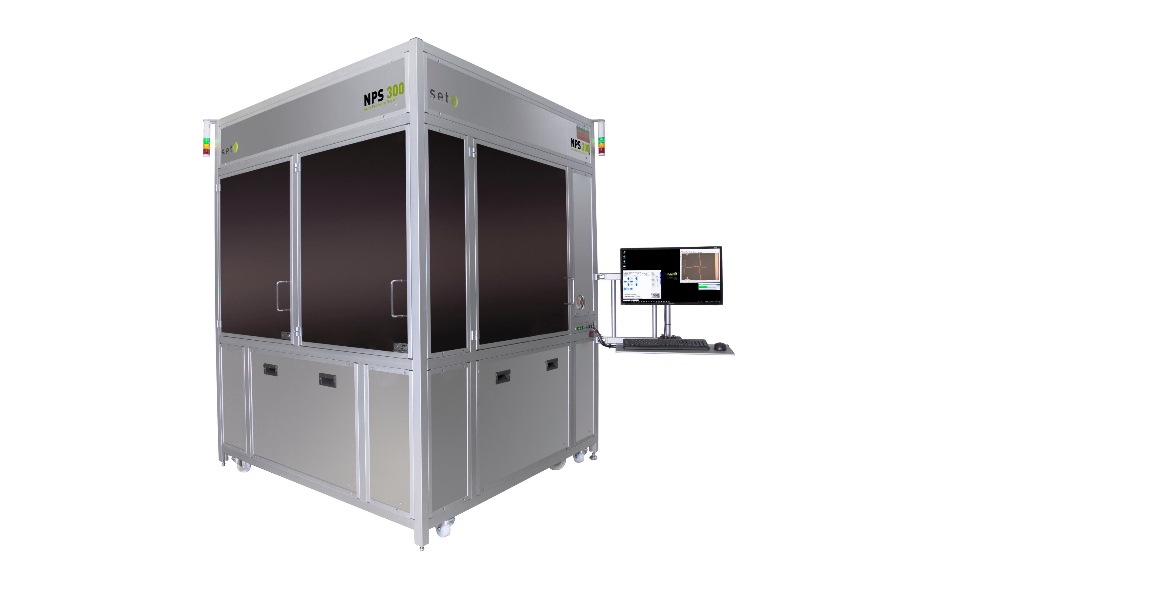
NPS300

-
工艺能力
用于热压印或紫外纳米压印光刻的步进和印模印刻技术是芬兰VTT技术研究中心已经验证过的创新方法。
- 热压印技术:该方法包括通过控制热量和压力将印模图案转印到热塑性压印材料中
- 紫外纳米压印光刻技术:是一种使用原位印刻配料以及紫外固化的步进和固化方法。当需要20纳米以下的分辨率时,这种尖端技术就成为了一种替代标准紫外光刻系统的非常有前景的解决方案。
-
应用
- 光子器件
- 高精度微光阵列和光栅
- CMOS-MEMS集成
- 高分辨率OLED显示器
- 用于移动存储的高密度HDD
- 其他新兴技术
-
纳米压印光刻技术
纳米结构的低成本生产方案正在开发中,这可能是半导体、MOEMS与光电子技术未来发展的驱动力。特别是,纳米压印光刻技术(NIL)及其变体已发展成为一种具有成本效益的技术,它可以替代高分辨率电子束光刻技术来印刷小于20纳米的几何形状。
印刻的原理是采用热或是紫外线固化工艺,使用带有纳米图案的印模对聚合物薄膜进行机械按压。带有图案的聚合物可以作为最终设备,例如成像传感器的透镜、微流控芯片、生物医学阵列等。它也可以作为一种高分辨率掩模应用于随后的工艺步骤中。
印刻是一种简单的光刻技术。它有三个基本的工艺步骤:
- 将印模与已预涂印刻材料的基板进行对准
- 将印模压入印刻材料以转印印模表面上的图案
- 将印模从印刻材料中分离出来
我们可以描述三种印刻或压印技术:热压印技术 (HEL),其使用热塑性材料;紫外纳米压印技术(UV-NIL),其使用液体抗蚀剂并在成型后用紫外光进行固化;以及软光刻技术,其使用冲压方法将预先在软印模上处理好的油墨转印到基板上。
Technicals papers associated
-
Optimizing indium bump deoxidation through 3D surface profilometry
MiNaPAD 2026
G. Chaumy
-
High Precision Die-to-Wafer Hybrid Bonding: Key Factors for Success
26-28 June 2023
P.Metzger
3D & Systems Summit, Dresden, Germany
-
Die to wafer hybrid bonding equipment: throughput versus precision
MiNaPAD 2022
SET, CEA Leti
-
Die-to-Wafer Direct Bonding for Production Environment with a New Flip-Chip Bonder
MiNaPAD 2019
P. Metzger, N. Raynaud
-
Flip-chip bonding: how to meet the high accuracy requirements ?
EMPC 2017
C. Avrillier
-
Toward a Flip-Chip Bonder dedicated to Direct Bonding for Production Environment
IWLPC 2017
SET, Saint-Jeoire, France
3D vertical integration of components is now an industrial reality. Considerations and results on direct bonding for HVM precise assembly are presented.
-
-
Considerations on the design of high precision Flip-Chip Bonder for mass production
European 3D Summit 2016
N. Raynaud
-
Results of the 2015 testbeam of 180 nm AMS High-Voltage CMOS sensor prototype
June 30, 2016
DPNC, University of Geneva, Switzerland
-
Evaluation of Sn-based Microbumping Technology for Hybrid IR Detectors, 10µm Pitch to 5µm Pitch
ECTC 2015
IMEC Leuven, Belgium SOFRADIR Veurey-Voroize, France
-
Flip-Chip Assembly for Focal Plane Array
ORION – Moscow International Conference Photoelectronics and Night Vision Devices 2014
J.-S. Mottet
-
Flip-chip assembly for focal plane array
IST:GST Mumbai 2017
P. Metzger
-
Development done on Device Bonder to address 3D requirements in a Production Environment
IWLPC 2014
SET, Saint-Jeoire, France
Key to the success of 3D integration will be the ability to accurately align and bond devices with aggressive feature sizes.
-
Die Attach Bonding using High-frequency Ultrasonic Energy for High-temperature application
June 2014
IME – Journal of Electronics materials (abstract)
-
Microbumping Technology for Hybrid IR detectors, 10µm pitch and beyond
EPTC 2014
IMEC Leuven, Belgium SOFRADIR Veurey-Voroize, France
Singapore
-
Interconnect and bonding techniques for pixelated X-ray and gamma-ray detectors
7-12 September, 2014
UNIVERSITY OF SURREY, Guilford, Surrey, U.K
10th International Conference on Position Sensitive Detectors
-
Aluminum to aluminum Bonding at Room Temperature
ECTC 2013
CEA – LETI, MINATEC Campus
-
Micro-tube insertion into aluminum pads: Simulation and experimental validations
IMAPS 2013
CEA – LETI, MINATEC Campus
9th International Conference and Exhibition on Device Packaging
This material is posted here with permission of IMAPS.
-
Chip to wafer copper direct bonding electrical characterization and thermal cycling
December 2013
CEA – LETI, MINATEC Campus
-
Die-to-Die and Die-to-Wafer Bonding solution for High Density, Fine Pitch Micro-Bumped Die
IMAPS Device Packaging Conference 2012
G. Lecarpentier
-
Chip to wafer direct bonding technologies for high density 3D integration
ECTC 2012
CEA – LETI, MINATEC, STMicroelectronics, SET
-
NaPANIL “Library of Processes”
March 2012
NaPANIL
Second edition with results of the NaPANIL-project
-
Chip-to-Wafer Technologies for High Density 3D Integration
MiNaPAD 2011
CEA Leti, Minatec campus, CNRS Cemes, ALES, SET, ST Microelectronics
-
Process and Equipment Enhancements for C2W bonding in a 3D Integration Scheme
IWLPC 2011
K. Cooper from SET North America
-
3D-IC Integration using D2C or D2W Alignment Schemes together with Local Oxide Reduction
IMAPS Device Packaging Conference 2011
G. Lecarpentier
-
Low-Profile 3D Silicon-on-Silicon Multi-chip Assembly
ECTC 2011
IBM T.J. Watson Research Center
This material is posted here with permission of IEEE.
-
A 10 μm Pitch Interconnection Technology using Micro Tube Insertion into Al-Cu for 3D Applications
ECTC 2011
CEA – LETI, MINATEC, LEM3 –CNRS/UPV-M
This material is posted here with permission of IEEE.
-
Flip-chip die bonding: an enabling technology for 3D integration
IWLPC 2010
K. Cooper from SET North America
-
Die-to-wafer bonding of thin dies using a 2-step approach: high accuracy placement, then gang bonding
IMAPS Device Packaging Conference 2010
G. Lecarpentier
-
Low Temperature Bonding of High Density Large Area Array Interconnects for 3D Integration
IMAPS 2010
RTI International
-
Embedded active device packaging technology for real DDR2 memory chips
IWLPC 2010
Industrial Technology Research Institute (ITRI)
Originally published in the IWLPC Proceedings
-
SET Technical Bulletin N°3
February 2010
CEA-Leti, IMEC, ITRI, IME-A*Star, RTI, etc…
-
Fabrication and performance of InAs/GaSb-based superlattice LWIR detectors
SPIE Defense, Sensing & Security 2010
HRL Laboratories
Copyright 2010 SPIE
-
Ultrathin 3D ACA FlipChip-In-Flex Technology
ECTC 2010
Berlin Technical University, NB Technologies and Fraunhofer IZM
This material is posted here with permission of IEEE.
-
Three Chips Stacking with Low Volume Solder Using Single Re-Flow Process
ECTC 2010
Institute of Microelectronics – A*STAR
This material is posted here with permission of IEEE.
-
Insertion Bonding: A Novel Cu-Cu Bonding Approach for 3D Integration
ECTC 2010
IMEC and the Katholieke Universiteit Leuven
This material is posted here with permission of IEEE.
-
RF MEMS and flip-chip for space flight demonstrator
June 2009
Thales Alenia Space
-
Electrical characterization of high count, 10 µm pitch, room-temperature vertical interconnections
Device Packaging 2009
CEA-LETI
This material is posted here with permission of Imaps.
-
New Reflow Soldering and Tip in Buried Box (TB2) Techniques For Ultrafine Pitch Megapixels Imaging Array
ECTC 2008
CEA-LETI
This material is posted here with permission of IEEE.