
ACCµRA OPTO

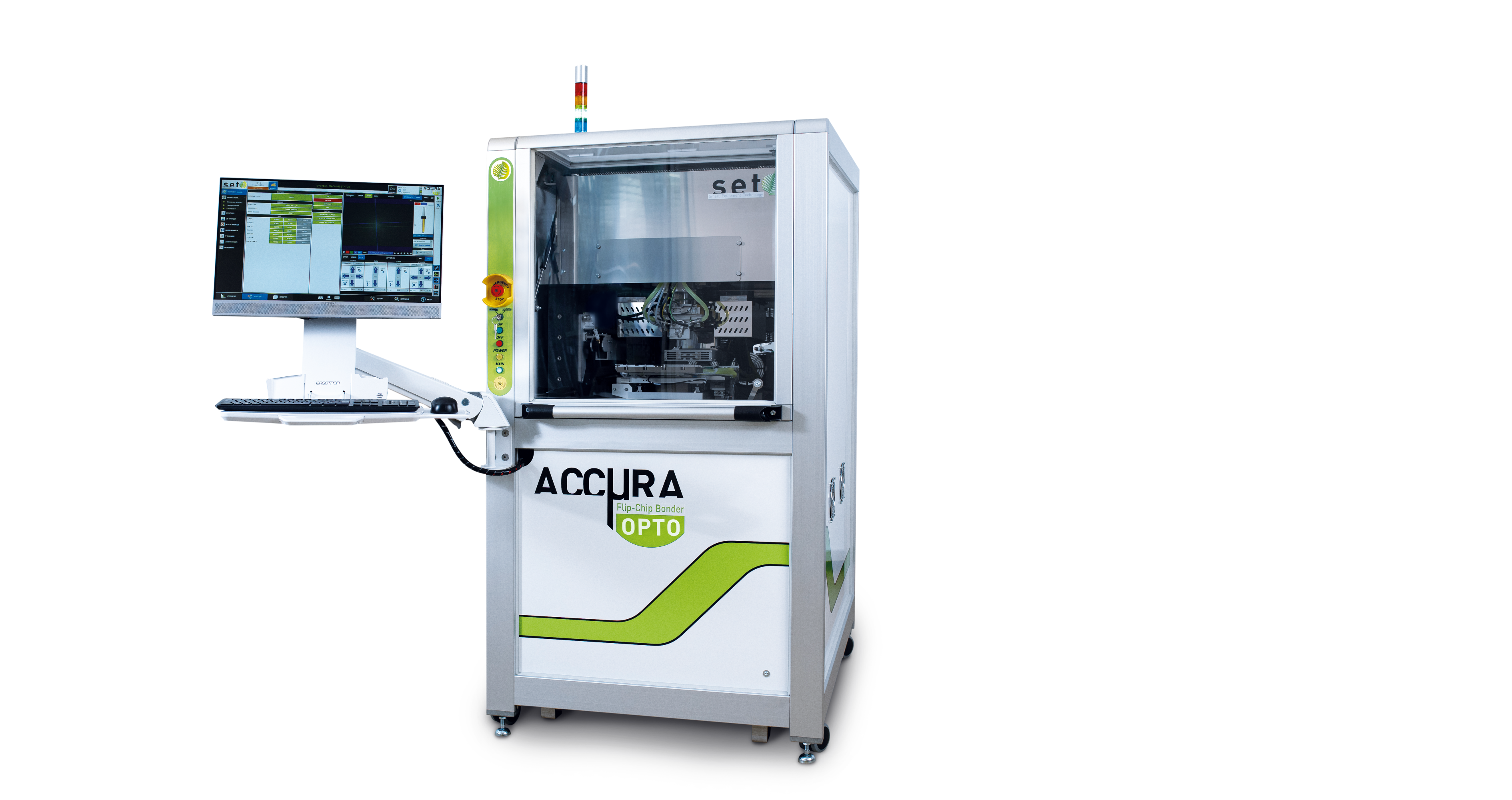
L’ACCµRA OPTO est un Flip-Chip Bonder permettant d’atteindre une précision post-assemblage de ± 0.5 µm.
Il est dédié aux procédés à faible force et de refusion. Les axes motorisés garantissent une haute répétabilité.
L’ACCµRA OPTO combine haute précision, flexibilité et accessibilité.
C’est l’équipement idéal pour l’optoélectronique et les applications photoniques sur silicium.
Request the technical paper
-
Avantages
- Précision post-assemblage de ± 0.5 µm
- Faible encombrement
- Facile d’utilisation
- Mise au point rapide
- Orientée R&D
- Faible force
-
Procédés
- Thermocompression
- Refusion
- Polymérisation UV
- Au, Au/Sn, In, Cu, Cu/Sn
-
Applications
- Flip-Chip, report de puces
- Puce-à-puce
- Puce-sur-wafer
- Optoélectronique
- Photonique
- MEMS, MOEMS, MCM
Technicals papers associated
-
Optimizing indium bump deoxidation through 3D surface profilometry
MiNaPAD 2026
G. Chaumy
-
High Precision Die-to-Wafer Hybrid Bonding: Key Factors for Success
26-28 June 2023
P.Metzger
3D & Systems Summit, Dresden, Germany
-
Die to wafer hybrid bonding equipment: throughput versus precision
MiNaPAD 2022
SET, CEA Leti
-
Die-to-Wafer Direct Bonding for Production Environment with a New Flip-Chip Bonder
MiNaPAD 2019
P. Metzger, N. Raynaud
-
Flip-chip bonding: how to meet the high accuracy requirements ?
EMPC 2017
C. Avrillier
-
Toward a Flip-Chip Bonder dedicated to Direct Bonding for Production Environment
IWLPC 2017
SET, Saint-Jeoire, France
3D vertical integration of components is now an industrial reality. Considerations and results on direct bonding for HVM precise assembly are presented.
-
-
Considerations on the design of high precision Flip-Chip Bonder for mass production
European 3D Summit 2016
N. Raynaud
-
Results of the 2015 testbeam of 180 nm AMS High-Voltage CMOS sensor prototype
June 30, 2016
DPNC, University of Geneva, Switzerland
-
Evaluation of Sn-based Microbumping Technology for Hybrid IR Detectors, 10µm Pitch to 5µm Pitch
ECTC 2015
IMEC Leuven, Belgium SOFRADIR Veurey-Voroize, France
-
Flip-Chip Assembly for Focal Plane Array
ORION – Moscow International Conference Photoelectronics and Night Vision Devices 2014
J.-S. Mottet
-
Flip-chip assembly for focal plane array
IST:GST Mumbai 2017
P. Metzger
-
Development done on Device Bonder to address 3D requirements in a Production Environment
IWLPC 2014
SET, Saint-Jeoire, France
Key to the success of 3D integration will be the ability to accurately align and bond devices with aggressive feature sizes.
-
Die Attach Bonding using High-frequency Ultrasonic Energy for High-temperature application
June 2014
IME – Journal of Electronics materials (abstract)
-
Microbumping Technology for Hybrid IR detectors, 10µm pitch and beyond
EPTC 2014
IMEC Leuven, Belgium SOFRADIR Veurey-Voroize, France
Singapore
-
Interconnect and bonding techniques for pixelated X-ray and gamma-ray detectors
7-12 September, 2014
UNIVERSITY OF SURREY, Guilford, Surrey, U.K
10th International Conference on Position Sensitive Detectors
-
Aluminum to aluminum Bonding at Room Temperature
ECTC 2013
CEA – LETI, MINATEC Campus
-
Micro-tube insertion into aluminum pads: Simulation and experimental validations
IMAPS 2013
CEA – LETI, MINATEC Campus
9th International Conference and Exhibition on Device Packaging
This material is posted here with permission of IMAPS.
-
Chip to wafer copper direct bonding electrical characterization and thermal cycling
December 2013
CEA – LETI, MINATEC Campus
-
Die-to-Die and Die-to-Wafer Bonding solution for High Density, Fine Pitch Micro-Bumped Die
IMAPS Device Packaging Conference 2012
G. Lecarpentier
-
Chip to wafer direct bonding technologies for high density 3D integration
ECTC 2012
CEA – LETI, MINATEC, STMicroelectronics, SET
-
NaPANIL “Library of Processes”
March 2012
NaPANIL
Second edition with results of the NaPANIL-project
-
Chip-to-Wafer Technologies for High Density 3D Integration
MiNaPAD 2011
CEA Leti, Minatec campus, CNRS Cemes, ALES, SET, ST Microelectronics
-
Process and Equipment Enhancements for C2W bonding in a 3D Integration Scheme
IWLPC 2011
K. Cooper from SET North America
-
3D-IC Integration using D2C or D2W Alignment Schemes together with Local Oxide Reduction
IMAPS Device Packaging Conference 2011
G. Lecarpentier
-
Low-Profile 3D Silicon-on-Silicon Multi-chip Assembly
ECTC 2011
IBM T.J. Watson Research Center
This material is posted here with permission of IEEE.
-
A 10 μm Pitch Interconnection Technology using Micro Tube Insertion into Al-Cu for 3D Applications
ECTC 2011
CEA – LETI, MINATEC, LEM3 –CNRS/UPV-M
This material is posted here with permission of IEEE.
-
Flip-chip die bonding: an enabling technology for 3D integration
IWLPC 2010
K. Cooper from SET North America
-
Die-to-wafer bonding of thin dies using a 2-step approach: high accuracy placement, then gang bonding
IMAPS Device Packaging Conference 2010
G. Lecarpentier
-
Low Temperature Bonding of High Density Large Area Array Interconnects for 3D Integration
IMAPS 2010
RTI International
-
Embedded active device packaging technology for real DDR2 memory chips
IWLPC 2010
Industrial Technology Research Institute (ITRI)
Originally published in the IWLPC Proceedings
-
SET Technical Bulletin N°3
February 2010
CEA-Leti, IMEC, ITRI, IME-A*Star, RTI, etc…
-
Fabrication and performance of InAs/GaSb-based superlattice LWIR detectors
SPIE Defense, Sensing & Security 2010
HRL Laboratories
Copyright 2010 SPIE
-
Ultrathin 3D ACA FlipChip-In-Flex Technology
ECTC 2010
Berlin Technical University, NB Technologies and Fraunhofer IZM
This material is posted here with permission of IEEE.
-
Three Chips Stacking with Low Volume Solder Using Single Re-Flow Process
ECTC 2010
Institute of Microelectronics – A*STAR
This material is posted here with permission of IEEE.
-
Insertion Bonding: A Novel Cu-Cu Bonding Approach for 3D Integration
ECTC 2010
IMEC and the Katholieke Universiteit Leuven
This material is posted here with permission of IEEE.
-
RF MEMS and flip-chip for space flight demonstrator
June 2009
Thales Alenia Space
-
Electrical characterization of high count, 10 µm pitch, room-temperature vertical interconnections
Device Packaging 2009
CEA-LETI
This material is posted here with permission of Imaps.
-
New Reflow Soldering and Tip in Buried Box (TB2) Techniques For Ultrafine Pitch Megapixels Imaging Array
ECTC 2008
CEA-LETI
This material is posted here with permission of IEEE.
